


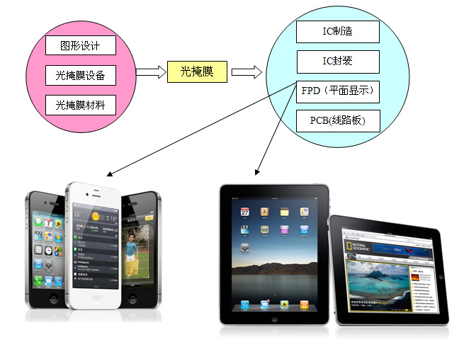
Photomasks are used in chip manufacturing, mainly IC (integrated circuit) chips, and are also used in the production of flat-panel displays, thin-film magnetic heads, and PC boards.
The photomask plays a role similar to that of a negative film to a photograph, and lithography is developed on the chip through the photomask. If the pattern is developed multiple times on both sides of the chip through a mask, this method is known as exposure, and the mask at this time can also be called a mask.
Chrome version is mainly used in:
TFT-LCD、CF、CSTN-LCD、STN-LCD、TN-LCD、EL、OLED、PDP、VFD等平板显示行业;
HDI, FPC and other printed circuit board industry;
IC Bumping, IC substrate, lead frame and other IC related industries;
Fine electronic components industries such as MENS, SENSOR and ENODER.